- 您现在的位置:买卖IC网 > Sheet目录1996 > ICS570GI-01T (IDT, Integrated Device Technology Inc)IC MULTIPLIER/ZDB 8-MSOP
ICS557-01
PCI-EXPRESS GEN1 CLOCK SOURCE
PCIE
IDT PCI-EXPRESS GEN1 CLOCK SOURCE
6
ICS557-01
REV P 072512
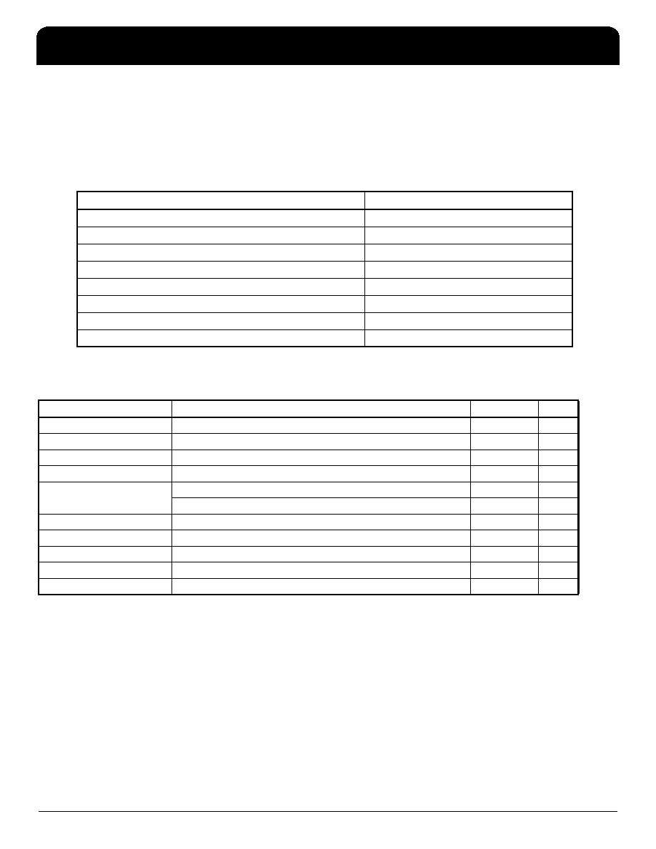
Absolute Maximum Ratings
Stresses above the ratings listed below can cause permanent damage to the ICS557-01. These ratings are stress
ratings only. Functional operation of the device at these or any other conditions above those indicated in the
operational sections of the specifications is not implied. Exposure to absolute maximum rating conditions for
extended periods can affect product reliability. Electrical parameters are guaranteed only over the recommended
operating temperature range.
DC Electrical Characteristics
Unless stated otherwise, VDD = 3.3 V ±5%, Ambient Temperature -40 to +85
° C
1 Single edge is monotonic when transitioning through region.
2 Inputs with pull-ups/-downs are not included.
Item
Rating
Supply Voltage, VDD, VDDA
5.5 V
All Inputs and Outputs
-0.5 V to VDD+0.5 V
Ambient Operating Temperature (commercial)
0 to +70
° C
Ambient Operating Temperature (industrial)
-40 to +85
° C
Storage Temperature
-65 to +150
° C
Junction Temperature
125
° C
Soldering Temperature
260
° C
ESD Protection (Input)
2000 V min. (HBM)
Parameter
Symbol
Conditions
Min.
Typ.
Max.
Units
Supply Voltage
V
3.135
3.465
Input High Voltage1
VIH
2.0
VDD +0.3
V
Input Low Voltage1
VIL
VSS-0.3
0.8
V
Input Leakage Current2
IIL
0 < Vin < VDD
-5
5
μA
Operating Supply Current
IDD
With 50
Ω and 2 pF load
55
mA
IDDOE
OE =Low
35
mA
Input Capacitance
CIN
Input pin capacitance
7
pF
Output Capacitance
COUT
Output pin capacitance
6
pF
Pin Inductance
LPIN
5nH
Output Resistance
Rout
CLK outputs
3.0
k
Ω
Pull-up Resistor
RPUP
OE
60
k
Ω
发布紧急采购,3分钟左右您将得到回复。
相关PDF资料
ICS571MLFT
IC BUFFER ZD LOW PH/NOISE 8-SOIC
ICS601G-01LF
IC CLK MULTIPLIER 16-TSSOP
ICS601M-02ILFT
IC CLOCK MULTIPLIER 16-SOIC
ICS601R-25ILF
IC CLOCK MULTIPLIER 1:5 20-SSOP
ICS613MLF
IC CLOCK MULT LOW PHASE 16-SOIC
ICS650G-40ALFT
IC CLOCK ETHERNET SWITCH 16TSSOP
ICS650GI-44LF
IC CLK SYNTHESIZER 16-TSSOP
ICS650GI-47LF
IC CLK SYNTHESIZER 16-TSSOP
相关代理商/技术参数
ICS570M
制造商:ICS 制造商全称:ICS 功能描述:Multiplier and Zero Delay Buffer
ICS570MI
制造商:ICS 制造商全称:ICS 功能描述:Multiplier and Zero Delay Buffer
ICS570MIT
制造商:ICS 制造商全称:ICS 功能描述:Multiplier and Zero Delay Buffer
ICS570MT
制造商:ICS 制造商全称:ICS 功能描述:Multiplier and Zero Delay Buffer
ICS571
制造商:ICS 制造商全称:ICS 功能描述:Low Phase Noise Zero Delay Buffer
ICS571M
功能描述:IC MULTIPLIER/ZDB 8-SOIC RoHS:否 类别:集成电路 (IC) >> 时钟/计时 - 时钟发生器,PLL,频率合成器 系列:ClockBlocks™ 产品变化通告:Product Discontinuation 04/May/2011 标准包装:96 系列:- 类型:时钟倍频器,零延迟缓冲器 PLL:带旁路 输入:LVTTL 输出:LVTTL 电路数:1 比率 - 输入:输出:1:8 差分 - 输入:输出:无/无 频率 - 最大:133.3MHz 除法器/乘法器:是/无 电源电压:3 V ~ 3.6 V 工作温度:0°C ~ 70°C 安装类型:表面贴装 封装/外壳:16-TSSOP(0.173",4.40mm 宽) 供应商设备封装:16-TSSOP 包装:管件 其它名称:23S08-5HPGG
ICS571MLF
功能描述:IC ZDB LOW PHASE NOISE 8-SOIC RoHS:是 类别:集成电路 (IC) >> 时钟/计时 - 时钟发生器,PLL,频率合成器 系列:ClockBlocks™ 标准包装:2,000 系列:- 类型:PLL 频率合成器 PLL:是 输入:晶体 输出:时钟 电路数:1 比率 - 输入:输出:1:1 差分 - 输入:输出:无/无 频率 - 最大:1GHz 除法器/乘法器:是/无 电源电压:4.5 V ~ 5.5 V 工作温度:-20°C ~ 85°C 安装类型:表面贴装 封装/外壳:16-LSSOP(0.175",4.40mm 宽) 供应商设备封装:16-SSOP 包装:带卷 (TR) 其它名称:NJW1504V-TE1-NDNJW1504V-TE1TR
ICS571MLFT
功能描述:IC BUFFER ZD LOW PH/NOISE 8-SOIC RoHS:是 类别:集成电路 (IC) >> 时钟/计时 - 时钟发生器,PLL,频率合成器 系列:ClockBlocks™ 标准包装:2,000 系列:- 类型:PLL 时钟发生器 PLL:带旁路 输入:LVCMOS,LVPECL 输出:LVCMOS 电路数:1 比率 - 输入:输出:2:11 差分 - 输入:输出:是/无 频率 - 最大:240MHz 除法器/乘法器:是/无 电源电压:3.135 V ~ 3.465 V 工作温度:0°C ~ 70°C 安装类型:表面贴装 封装/外壳:32-LQFP 供应商设备封装:32-TQFP(7x7) 包装:带卷 (TR)